Every now and then, I come across a tech development that makes me feel like I’m living in the future, and this is one of those moments. A team of scientists at Fudan University in Shanghai have published a study detailing their latest achievement, a fully functional memory chip built with integrated 2D materials a few atoms thick. Yesssss. This is the Star Trek-level technology I was promised as a child.
Well, maybe that’s jumping the gun a bit. Still, the achievement here is incredibly impressive (via Tom’s Hardware). Essentially, the researcher’s new Atom2chip process allowed them to flow a layer of molybdenum disulphide, functioning as a memory array, on top of a 0.13 micrometre CMOS silicon chip—fusing together an emerging atomic-scale, “2D” technology with traditional methods to create a working hybrid memory chip.
The chip-riding 2D flash memory array is able to communicate with the CMOS chip’s control logic via a custom interface, which in turn means that instruction-driven operations, 32-bit parallelism and random access instructions can be swapped between the two.
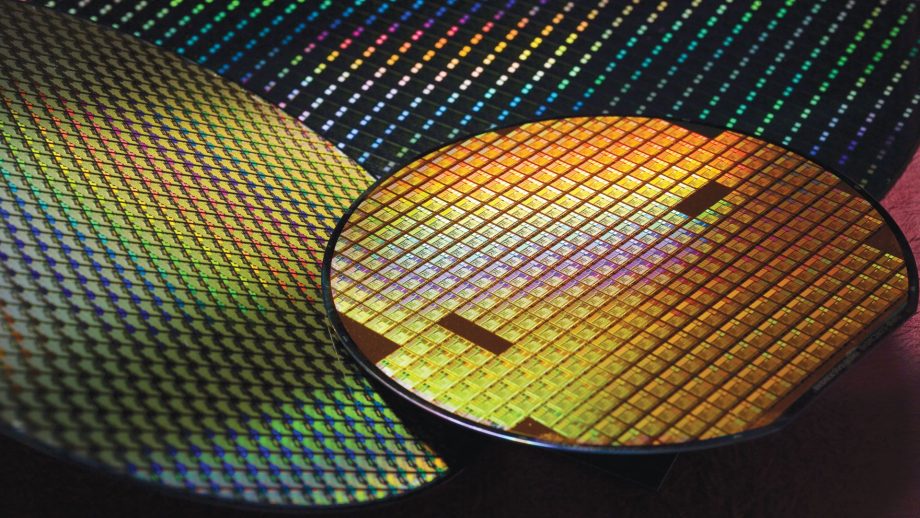
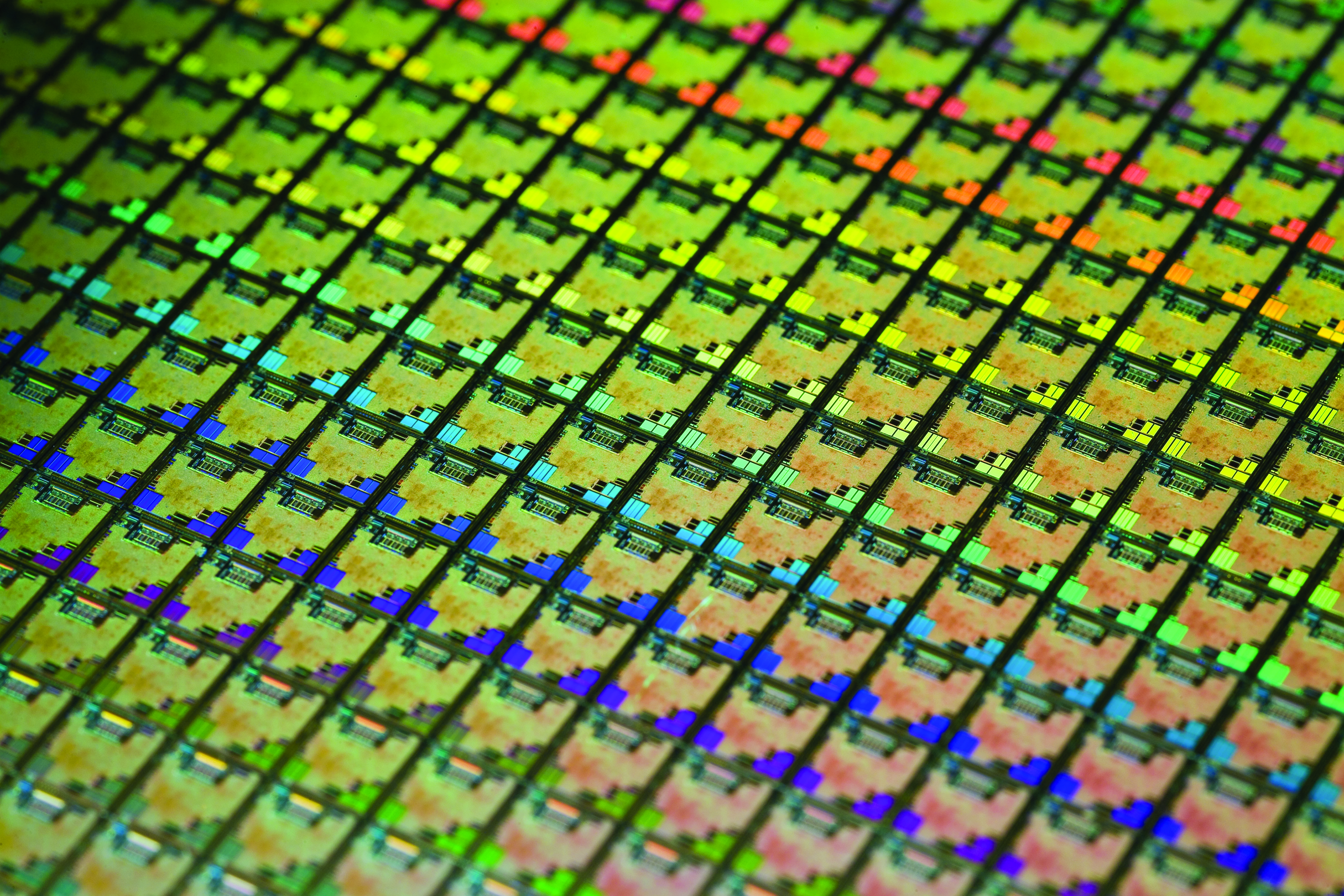
And the deeper you go, the more impressive the scale of the achievement becomes. While wafers are polished as part of the production process, they’ve still got a layer of uneven terrain (we’re talking nano-level, here) that could otherwise tear a several-atom-thick layer into an unworkable mess.


